Products application

Thin film photovoltaic
Flat display industry
Low-e glass industry
Optical coating industry
Tools coating industry
Semiconductor industry
Rare-Earth Permanent industry
Electrochromis industry
current location:Home > Products application > Semiconductor industry
     Semiconductor produce process include crystal circle making,crastal circle testing,chip packing and ending test .after encapsulation,its need a series of other process.such as:Post Mold Cure、Trim&Form、Plating and printing process etc. Typical encapsulation process is scribing/Loading/ bonding/Sealing/edging / electroplating/printing/ tendon-cut and molding/ inspection/testing/shipping.In the whole manufacturing ,  sputtering process was existed in Crystal making and chip packaging.

     APG in Semiconductor  indusrty to provide target material basically has:

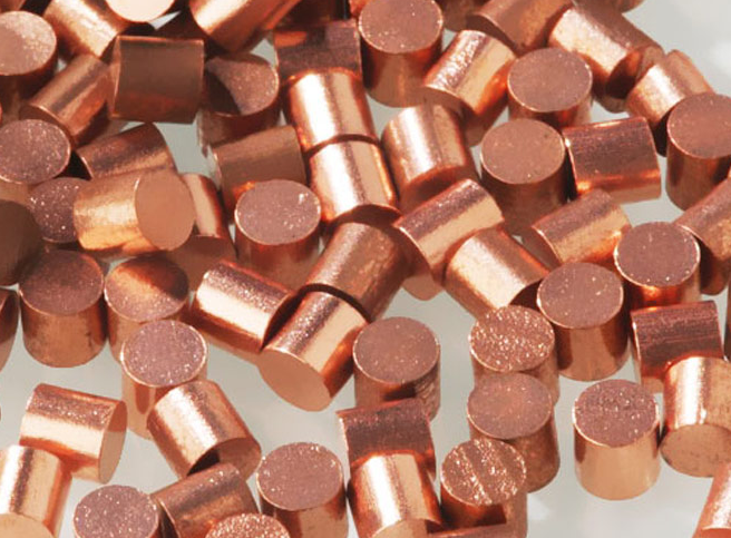
Type ltem Descripetion Purity Technology
Purity-Targets Cu
acc. your require 99.99% melting
Ti
99.99%
melting、CIP
W
99.99%
sintering、HIP
SS

melting
Al
99.99%
melting
Si
99.99%
pulled crystal+spraying+sintering
Mo 99.99%
sintering
Cr
99.99%
HIP、spraying
Ta
99.99%
melting
Ag 99.99%
melting
Pt
99.9%
melting
Ir
99.99%
melting
Sc
99.95%
melting
In
99.99%
cast
Aolly-Targets
AlSc
99.8%-99.99%
sintering
NiFe
99.9%-99.999%
spraying
NiCr
99.95%
meltingspraying
NiCu
99.95%
melting
NiV
99.95%
melting
WTi
99.9%
meltingspraying
Evaporation material

Cu、Ti、W、Al、Mo、Cr、Ta、Ag、Au、Pt、Ir、Y